OPTICALLY MONITORING AND CONTROLLING NANOSCALE TOPOGRAPHY DURING SEMICONDUCTOR ETCHING, NATURE-LIGHT: SCIENCE & APPLICATIONS, 1, E30 (2012)
C. EDWARDS, A. ARBABI, G. POPESCU, AND L. GODDARD
2012
![]()
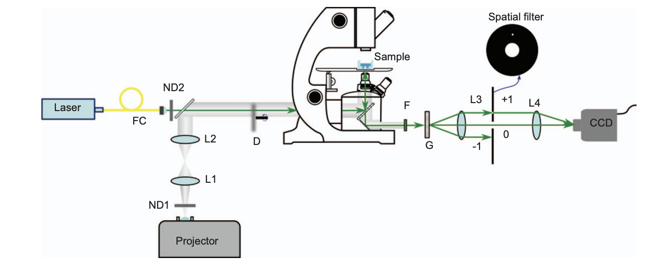
We present epi-diffraction phase microscopy (epi-DPM) as a non-destructive optical method for monitoring semiconductor fabrication processes in real time and with nanometer level sensitivity. The method uses a compact Mach–Zehnder interferometer to recover quantitative amplitude and phase maps of the field reflected by the sample. The low temporal noise of 0.6 nm per pixel at 8.93 frames per second enabled us to collect a three-dimensional movie showing the dynamics of wet etching and thereby accurately quantify non-uniformities in the etch rate both across the sample and over time. By displaying a gray-scale digital image on the sample with a computer projector, we performed photochemical etching to define arrays of microlenses while simultaneously monitoring their etch profiles with epi-DPM.