Detecting 20 NM Wide Defects in Large Area Nanopatterns Using Optical Interferometric Microscopy
Zhou R, Edwards C, Arbabi A, Popescu G, Goddard LL
Nano Letters 2013 13(8) 3716 https://doi.org/10.1021/nl401622b
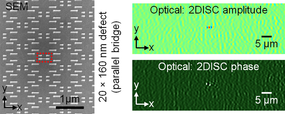
Due to the diffraction limited resolution and the presence of speckle noise, visible laser light is generally thought to be impractical for finding deep subwavelength defects in patterned semiconductor wafers. Here, we report on a nondestructive low-noise interferometric imaging method capable of detecting nanoscale defects within a wide field of view using visible light. The method uses a common-path laser interferometer and a combination of digital image processing techniques to produce 70 μm by 27 μm panoramic phase and amplitude images of the test nanopattern. Significant noise reduction and high sensitivity are achieved, which enables successful detection of several different types of sparse defects with sizes on the order of 20 nm wide by 100 nm long by 110 nm tall.